����ģ��ת����(ADC)��INL/DNL���� - ��ģ��� -
����ģ��ת����(ADC)��INL/DNL����
Abstract: Although integral and differential nonlinearity may not be the most important parameters for high-speed, high dynamic performance data converters, they gain significance when it comes to high-resolution imaging applications. The following application note serves as a refresher course for their definitions and details two different, yet commonly used techniques to measure INL and DNL in high-speed analog-to-digital converters (ADCs).
Manufacturers have recently introduced high-performance analog-to-digital converters (ADCs) that feature outstanding static and dynamic performance. You might ask, "How do they measure this performance, and what equipment is used?" The following discussion should shed some light on techniques for testing two of the accuracy parameters important for ADCs: integral nonlinearity (INL) and differential nonlinearity (DNL).
Although INL and DNL are not among the most important electrical characteristics that specify the high-performance data converters used in communications and fast data-acquisition applications, they gain significance in the higher-resolution imaging applications. However, unless you work with ADCs on a regular basis, you can easily forget the exact definitions and importance of these parameters. The next section therefore serves as a brief refresher course.
INL and DNL Definitions
DNL error is defined as the difference between an actual step width and the ideal value of 1LSB (see Figure 1a). For an ideal ADC, in which the differential nonlinearity coincides with DNL = 0LSB, each analog step equals 1LSB (1LSB = VFSR/2N, where VFSR is the full-scale range and N is the resolution of the ADC) and the transition values are spaced exactly 1LSB apart. A DNL error specification of less than or equal to 1LSB guarantees a monotonic transfer function with no missing codes. An ADC's monotonicity is guaranteed when its digital output increases (or remains constant) with an increasing input signal, thereby avoiding sign changes in the slope of the transfer curve. DNL is specified after the static gain error has been removed. It is defined as follows:
DNL = |[(VD+1- VD)/VLSB-IDEAL - 1] | , where 0 < D < 2N - 2.
VD is the physical value corresponding to the digital output code D, N is the ADC resolution, and VLSB-IDEAL is the ideal spacing for two adjacent digital codes. By adding noise and spurious components beyond the effects of quantization, higher values of DNL usually limit the ADC's performance in terms of signal-to-noise ratio (SNR) and spurious-free dynamic range (SFDR).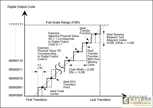
Figure 1a. To guarantee no missing codes and a monotonic transfer function, an ADC's DNL must be less than 1LSB.
INL error is described as the deviation, in LSB or percent of full-scale range (FSR), of an actual transfer function from a straight line. The INL-error magnitude then depends directly on the position chosen for this straight line. At least two definitions are common: "best straight-line INL" and "end-point INL" (see Figure 1b):
- Best straight-line INL provides information about offset (intercept) and gain (slope) error, plus the position of the transfer function (discussed below). It determines, in the form of a straight line, the closest approximation to the ADC's actual transfer function. The exact position of the line is not clearly defined, but this approach yields the best repeatability, and it serves as a true representation of linearity.
- End-point INL passes the straight line through end points of the converter's transfer function, thereby defining a precise position for the line. Thus, the straight line for an N-bit ADC is defined by its zero (all zeros) and its full-scale (all ones) outputs.
The best straight-line approach is generally preferred, because it produces better results. The INL specification is measured after both static offset and gain errors have been nullified, and can be described as follows:
INL = | [(VD - VZERO)/VLSB-IDEAL] - D | , where 0 < D < 2N-1.
VD is the analog value represented by the digital output code D, N is the ADC's resolution, VZERO is the minimum analog input corresponding to an all-zero output code, and VLSB-IDEAL is the ideal spacing for two adjacent output codes.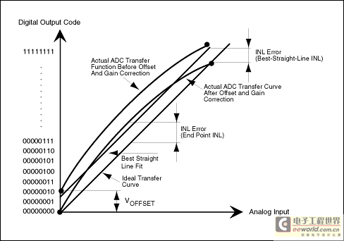
Figure 1b. Best straight-line and end-point fit are two possible ways to define the linearity characteristic of an ADC.
Transfer Function
The transfer function for an ideal ADC is a staircase in which each tread represents a particular digital output code and each riser represents a transition between adjacent codes. The input voltages corresponding to these transitions must be located to specify many of an ADC's performance parameters. This chore can be complicated, especially for the noisy transitions found in high-speed converters and for digital codes that are near the final result and changing slowly.
Transitions are not sharply defined, as shown in Figure 1b, but are more realistically presented as a probability function. As the slowly increasing input voltage passes through a transition, the ADC converts more and more frequently to the next adjacent code. By definition, the transition corresponds to that input voltage for which the ADC converts with equal probability to each of the flanking codes.
The Right Transition A transition voltage is defined as the input voltage that has equal probabilities of generating either of the two adjacent codes. The nominal analog value, corresponding to the digital output code generated by an analog input in the range between a pair of adjacent transitions, is defined as the midpoint (50% point) of this range. If the limits of the transition interval are known, this 50% point is calculated easily. The transition point can be determined at test by measuring the limits of the transition interval, and then dividing the interval by the number of times each of the adjacent codes appears within it.
Generic Setup for Testing Static INL and DNL
INL and DNL can be measured with either a quasi-DC voltage ramp or a low-frequency sine wave as the input. A simple DC (ramp) test can incorporate a logic analyzer, a high-accuracy DAC (optional), a high-precision DC source for sweeping the input range of the device under test (DUT), and a control interface to a nearby PC or X-Y plotter.
If the setup includes a high-accuracy DAC (much higher than that of the DUT), the logic analyzer can monitor offset and gain errors by processing the ADC's output data directly. The precision signal source creates test voltages for the DUT by sweeping slowly through the input range of the ADC from zero scale to full scale. Once reconstructed by the DAC, each test voltage at the ADC input is subtracted from its corresponding DC level at the DAC output, producing a small voltage difference (VDIFF) that can be displayed with an X-Y plotter and linked to the INL and DNL errors. A change in quantization level indicates differential nonlinearity, and a deviation of VDIFF from zero indicates the presence of integral nonlinearity.
Analog Integrating Servo Loop
Another way to determine static linearity parameters for an ADC, similar to the preceding but more sophisticated, is using an analog integrating servo loop. This method is usually reserved for test setups that focus on high-precision measurements rather than speed.
A typical analog servo loop (see Figure 2) consists of an integrator and two current sources connected to the ADC input. One source forces a current into the integrator, and the other serves as a current sink. A digital magnitude comparator connected to the ADC output controls both current sources. The other input of the magnitude comparator is controlled by a PC, which sweeps it through the 2N - 1 test codes for an N-bit converter.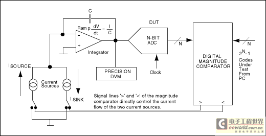
Figure 2. This circuit configuration is an analog integrating servo loop.
If the polarity of feedback around the loop is correct, the magnitude comparator causes the current sources to servo the analog input around a given code transition. Ideally, this action produces a small triangular wave at the analog inputs. The magnitude comparator controls both rate and direction for these ramps. The integrator's ramp rate must be fast when approaching a transition, yet sufficiently slow to minimize peak excursions of the superimposed triangular wave when measuring with a precision digital voltmeter (DVM).
For INL/DNL tests on the MAX108, the servo-loop board connects to the evaluation board through two headers (see Figure 3). One header establishes a connection between the MAX108's primary (or auxiliary) output port and the magnitude comparator's latchable input port (P). The second header ensures a connection between the servo loop (the magnitude comparator's Q port) and a computer-generated digital reference code.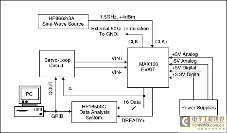
Figure 3. With the aid of the MAX108EVKIT and an analog integrating servo loop, this test setup determines the MAX108's INL and DNL characteristics.
The fully decoded decision resulting from this comparison is available at the comparator output P > QOUT, and is then passed on to the integrator configurations. Each comparator result controls the logic input of the switch independently and generates voltage ramps as required to drive succeeding integrator circuits for both inputs of the DUT. This approach has its advantages, but it also has several drawbacks:
- The triangular ramp should have low dV/dt to minimize noise. This condition generates repeatable numbers, but it results in long integration times for the precision meter.
- Positive and negative ramp rates must be matched to arrive at the 50% point, and the low-level triangular waves must be averaged to achieve the desired DC level.
- Integrator designs usually require careful selection of the charge capacitors. To minimize potential errors due to the capacitors' "memory effect," for instance, select integrator capacitors with low dielectric absorption.
- Accuracy is proportional to the i
�������������������������� �鿴���� �ظ�
"����ģ��ת����(ADC)��INL/DNL���� - ��ģ��� -"���������
��������
- ģ�⼯�ɵ�·�IJ��Լ���-ģ�����-
- ��γ�Ϊ��ɫ��ģ���ʦ:���ָ�����ģ�����-ģ���
- ���ģ�������MEMS��˷��������-ģ�����-
- �����¶ȼƵ�ģ�ⲿ�ֵ�·ͼ-ģ�����-
- �����ⲿ�ж�ʵ��ģ������ݵ��շ�-ģ�����-
- ������/�����̻���ɡ�ģ��뵼��ӭ��ɳ�������-ģ��
- TI�߾���ʵ�������߿γ� �����ɫ����ģ����ƴ���-ģ
- ģ��ʾ����������ʾ����������-ģ�����-
- ������PLC���ڷ�ģ�����������-ģ�����-
- �û���ź�ʾ����̽��ģ��������ź�-ģ�����-