�˽�ģ��ת��������Ӱ��ϵͳ����-Understanding - ��ģ��� -
��Դ�� �����û����������а�Ȩ��ϵ����ɾ����2018-09-29��
Using a 12-bit-resolution analog-to-digital converter (ADC) does not necessarily mean your system will have 12-bit accuracy. Sometimes, much to the surprise and consternation of engineers, a data-acquisition system will exhibit much lower performance than expected. When this is discovered after the initial prototype run, a mad scramble for a higher-performance ADC ensues, and many hours are spent reworking the design as the deadline for preproduction builds fast approaches. What happened? What changed from the initial analysis? A thorough understanding of ADC specifications will reveal subtleties that often lead to less-than-desired performance. Understanding ADC specifications will also help you in selecting the right ADC for your application.
We start by establishing our overall system-performance requirements. Each component in the system will have an associated error; the goal is to keep the total error below a certain limit. Often the ADC is the key component in the signal path, so we must be careful to select a suitable device. For the ADC, let's assume that the conversion-rate, interface, power-supply, power-dissipation, input-range, and channel-count requirements are acceptable before we begin our evaluation of the overall system performance. Accuracy of the ADC is dependent on several key specs, which include integral nonlinearity error (INL), offset and gain errors, and the accuracy of the voltage reference, temperature effects, and AC performance. It is usually wise to begin the ADC analysis by reviewing the DC performance, because ADCs use a plethora of nonstandardized test conditions for the AC performance, making it easier to compare two ICs based on DC specifications. The DC performance will in general be better than the AC performance.
System Requirements
Two popular methods for determining the overall system error are the root-sum-square (RSS) method and the worst-case method. When using the RSS method, the error terms are individually squared, then added, and then the square root is taken. The RSS error budget is given by:
where EN represents the term for a particular circuit component or parameter. This method is most accurate when the all error terms are uncorrelated (which may or may not be the case). With worst-case error analysis, all error terms add. This method guarantees the error will never exceed a specified limit. Sinceit sets the limit of how bad the error can be, the actual error is always less than this value (often-times MUCH less).
The measured error is usually somewhere between the values given by the two methods, but is often closer to the RSS value. Note that depending on one's error budget, typical or worst-case values for the error terms can be used. The decision is based on many factors, including the standard deviation of the measurement value, the importance of that particular parameter, the size of the error in relation to other errors, etc. So there really aren't hard and fast rules that must be obeyed. For our analysis, we will use the worst-case method.
In this example, let's assume we need 0.1% or 10 bits of accuracy (1/210), so it makes sense to choose a converter with greater resolution than this. If we select a 12-bit converter, we can assume it will be adequate; but without reviewing the specifications, there is no guarantee of 12-bit performance (it may be better or worse). For example, a 12-bit ADC with 4LSBs of integral nonlinearity error can give only 10 bits of accuracy at best (assuming the offset and gain errors have been calibrated). A device with 0.5LSBs of INL can give 0.0122% error or 13 bits of accuracy (with gain and offset errors removed). To calculate best-case accuracy, divide the maximum INL error by 2N, where N is the number of bits. In our example, allowing 0.075% error (or 11 bits) for the ADC leaves 0.025% error for the remainder of the circuitry, which will include errors from the sensor, the associated front-end signal conditioning circuitry (op amps, multiplexers, etc.), and possibly digital-to-analog converters (DACs), PWM signals, or other analog-output signals in the signal path.
We assume that the overall system will have a total-error budget based on the summation of error terms for each circuit component in the signal path. Other assumptions we will make are that we are measuring a slow-changing, DC-type, bipolar input signal with a 1kHz bandwidth and that our operating temperature range is 0��C to 70��C with performance guaranteed from 0��C to 50��C.
DC Performance
Differential nonlinearity
Though not mentioned as a key parameter for an ADC, the differential nonlinearity (DNL) error is the first specification to observe. DNL reveals how far a code is from a neighboring code. The distance is measured as a change in input-voltage magnitude and then converted to LSBs (Figure 1). Note that INL is the integral of the DNL errors, which is why DNL is not included in our list of key parameters. The key for good performance for an ADC is the claim "no missing codes." This means that, as the input voltage is swept over its range, all output code combinations will appear at the converter output. A DNL error of <��1LSB guarantees no missing codes (Figure 1a). In Figures 1b, 1c, and 1d, three DNL error values are shown. With a DNL error of -0.5LSB (Figure 1b), the device is guaranteed to have no missing codes. With a value equal to -1LSB (Figure 1c), the device is not necessarily guaranteed to have no missing codes. Note that code 10 is missing. However, most ADCs that specify a maximum DNL error of +/-1 will specifically state whether the device has missing codes or not. Because the production-test limits are actually tighter than the data-sheet limits, no missing codes is usually guaranteed. With a DNL value greater than -1 (-1.5LSB in Figure 1d), the device has missing codes.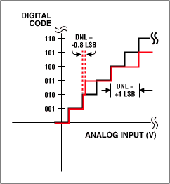
Figure 1a. DNL error: no missing codes.
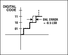
Figure 1b. DNL error: no missing codes.
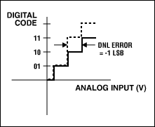
Figure 1c. DNL error: Code 10 is missing.
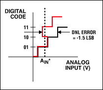
Figure 1d. DNL error: At AIN* the digital code can be one of three possible values. When the input voltage is swept, Code 10 will be missing.
When DNL-error values are offset (that is, -1LSB, +2LSB), the ADC transfer function is altered. Offset DNL values can still in theory have no missing codes. The key is having -1LSB as the low limit. Note that DNL is measured in one direction, usually going up the transfer function. The input-voltage level required to create the transition at code [N] is compared to that at code [N+1]. If the difference is 1LSB apart, the DNL error is zero. If it is greater than 1LSB, the DNL error is positive; if it is less than 1LSB, the DNL error is negative.
Having missing codes is not necessarily bad. If you need only 13 bits of resolution and you have a choice between a 16-bit ADC with a DNL specification < = +/-4LSB DNL (which is effectively 14 bits, no missing codes) that costs $5 and a 16-bit ADC with a DNL of < = +/-1LSB that costs $15, then buying the lower-grade version of the ADC will allow you to greatly reduce component cost and still meet your system requirements.
INL
INL is defined as the integral of the DNL errors, so good INL guarantees good DNL. The INL error tells how far away from the ideal transfer-function value the measured converter result is. Continuing with our example, an INL error of +/-2LSB in a 12-bit system means the maximum nonlinearity error may be off by 2/4096 or 0.05% (which is already about two-thirds of the allotted ADC error budget). Thus, a 1LSB (or better) part is required. With a +/-1LSB INL error, the accuracy is 0.0244%, which accounts for 32.5% of the allotted ADC error budget. With a specification of 0.5LSB, the accuracy is 0.012%, and this accounts for only about 16% (0.012%/0.075%) of our ADC error budget limit. Note that neither INL nor DNL errors can be calibrated or corrected easily.Offset and Gain Errors
Offset and gain errors can easily be calibrated out using a microcontroller (C) or a digital signal processor (DSP). With offset error, the measurement is simple when the converter allows bipolar input signals. In bipolar systems, offset error shifts the transfer function but does not reduce the number of available codes (Figure 2). There are two methodologies to zero out bipolar errors. In one, you shift the x and y axes of the transfer function so that the negative full-scale point aligns with the zero point of a unipolar system (Figure 3a). With this technique, you simply remove the offset error and then adjust for gain error by rotating the transfer function about the "new" zero point. The second technique entails using an iterative approach. First apply zero volts to the ADC input and perform a conversion; the conversion result represents the bipolar zero offset error. Then perform a gain adjustment by rotating the curve about the negative full-scale point (Figure 3b). Note that the transfer function has pivoted around point A, which moves the zero point away from the desired transfer function. Thus, a subsequent offset-error calibration may be required.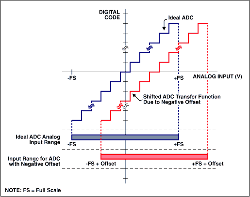
Figure 2. Bipolar offset error.
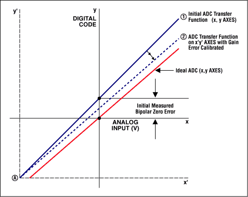
Figure 3a.
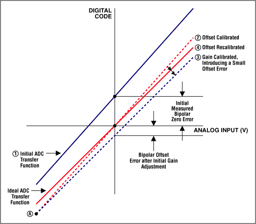
Figure 3b.
Figures 3a and 3b. Calibrating bipolar offset error. (Note: The stair-step transfer function has been replaced by a straight line, because this graph shows all codes and the step size is so small that the line appears to be linear.)
Unipolar systems are a little trickier. If the offset is positive, use the same methodology as that for bipolar supplies. The difference here is that you lose part of the ADC's range (see Figure 4). If the offset is negative, you cannot simply do a conversion and expect the result to represent the offset error. Below zero, the converter will just display zeros. Thus, with a negative offset error, you must increase the input voltage slowly to determine where the first ADC transition occurs. Here again you lose part of the ADC range.
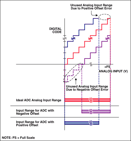
Figure 4. Unipolar offset error.
Returning to our example, two scenarios for offset error are given below:
�������������������������� �鿴���� �ظ�
"�˽�ģ��ת��������Ӱ��ϵͳ����-Understanding - ��ģ��� -"���������
��������
- ģ�⼯�ɵ�·�IJ��Լ���-ģ�����-
- ��γ�Ϊ��ɫ��ģ���ʦ:���ָ�����ģ�����-ģ���
- ���ģ�������MEMS��˷��������-ģ�����-
- �����¶ȼƵ�ģ�ⲿ�ֵ�·ͼ-ģ�����-
- �����ⲿ�ж�ʵ��ģ������ݵ��շ�-ģ�����-
- ������/�����̻���ɡ�ģ��뵼��ӭ��ɳ�������-ģ��
- TI�߾���ʵ�������߿γ� �����ɫ����ģ����ƴ���-ģ
- ģ��ʾ����������ʾ����������-ģ�����-
- ������PLC���ڷ�ģ�����������-ģ�����-
- �û���ź�ʾ����̽��ģ��������ź�-ģ�����-