����dsPIC33FJ��Ƶ�PSFBש��DC-DCת�������� - ģ���Դ -
���Ľ�����dsPIC33FJϵ����Ҫ���ԣ�����ͼ��CPU �˷���ͼ��DSP ���淽��ͼ������PFC��ͼ�Լ�����Ӧ�ÿ�ͼ���������������ȫ�ţ�PSFB�� 1/4ש��DC-DCת�����ο������Ҫ���Ժ�ָ�꣬��ϸ��·ͼ������嵥��BOM����
Microchip ��˾��dsPIC33FJ06GS101/X02��dsPIC33FJ16GSX02/X04�����й㷺��DSP���ܺ�����16λMCU�ܹ���3.0-3.6V�����ܴﵽ40MIPS������16λ��������ͨ·��24λ��ָ��㷺Ӧ����AC/DCת����������HID����س������DC/DCת�������������������¯����������Դ/�����Ҳ��������UPS��
dsPIC33FJϵ����Ҫ���ԣ�
Operating Range:
Up to 40 MIPS Operation (at 3.0-3.6V):
- Industrial temperature range (-40�� to +85��)
- Extended temperature range (-40�� to +125��)
High-Performance DSC CPU:
Modified Harvard Architecture
C Compiler Optimized Instruction Set
16-Bit Wide Data Path
24-Bit Wide Instructions
Linear Program Memory Addressing up to 4M Instruction Words
Linear Data Memory Addressing up to 64 Kbytes
83 Base Instructions: Mostly 1 Word/1 Cycle
Two 40-Bit Accumulators with Rounding and Saturation Options
Flexible and Powerful Addressing modes:
- Indirect
- Modulo
- Bit-Reversed
Software Stack
16 x 16 Fractional/Integer Multiply Operations
32/16 and 16/16 Divide Operations
Single-Cycle Multiply and Accumulate:
- Accumulator write back for DSP operations
- Dual data fetch
Up to ��16-Bit Shifts for up to 40-Bit Data
Digital I/
Peripheral Pin Select Functionality
Up to 35 Programmable Digital I/O Pins
Wake-up/Interrupt-on-Change for up to 30 Pins
Output Pins can Drive Voltage from 3.0V to 3.6V
Up to 5V Output with Open-Drain Configuration
5V Tolerant Digital Input Pins (except RB5)
16 mA Source/Sink on All PWM pins
On-Chip Flash and SRAM:
Flash Program Memory (up to 16 Kbytes)
Data SRAM (up to 2 Kbytes)
Boot and General Security for Program Flash
Peripheral Features:
Timer/Counters, up to Three 16-Bit Timers:
- Can pair up to make one 32-bit timer
Input Capture (up to two channels):
- Capture on up, down or both edges
- 16-bit capture input functions
- 4-deep FIFO on each capture
Output Compare (up to two channels):
- Single or Dual 16-Bit Compare mode
- 16-Bit Glitchless PWM mode
4-Wire SPI:
- Framing supports I/O interface to simple codecs
- 1-deep FIFO Buffer.
- Supports 8-bit and 16-bit data
- Supports all serial clock formats and sampling modes
I2C:
- Supports Full Multi-Master Slave mode
- 7-bit and 10-bit addressing
- Bus collision detection and arbitration
- Integrated signal conditioning
- Slave address masking
UART:
- Interrupt on address bit detect
- Interrupt on UART error
- Wake-up on Start bit from Sleep mode
- 4-character TX and RX FIFO buffers
- LIN bus support
- IrDA encoding and decoding in hardware
- High-Speed Baud mode
- Hardware Flow Control with CTS and RTS
Interrupt Controller:
5-Cycle Latency
Up to 35 Available Interrupt Sources
Up to Three External Interrupts
Seven Programmable Priority Levels
Four Processor Exceptions
High-Speed PWM Module Features:
Up to Four PWM Generators with Four to Eight Outputs
Individual Time Base and Duty Cycle for each of the Eight PWM Outputs
Dead Time for Rising and Falling Edges
Duty Cycle Resolution of 1.04 ns
Dead-Time Resolution of 1.04 ns
Phase Shift Resolution of 1.04 ns
Frequency Resolution of 1.04 ns
PWM modes Supported:
- Standard Edge-Aligned
- True Independent Output
- Complementary
- Center-Aligned
- Push-Pull
- Multi-Phase
- Variable Phase
- Fixed Off-Time
- Current Reset
- Current-Limit
Independent Fault/Current-Limit Inputs for 8 PWM Outputs
Output Override Control
Special Event Trigger
PWM Capture Feature
Prescaler for Input Clock
Dual Trigger from PWM to ADC
PWMxL, PWMxH Output Pin Swapping
PWM4H, PWM4L Pins Remappable
On-the-Fly PWM Frequency, Duty Cycle and Phase Shift Changes
Disabling of Individual PWM Generators
Leading-Edge Blanking (LEB) Functionality
High-Speed Analog Comparator
Up to Four Analog Comparators:
- 20 ns response time
- 10-bit DAC for each analog comparator
- DACOUT pin to provide DAC output
- Programmable output polarity
- Selectable input source
- ADC sample and convert capability
PWM Module Interface:
- PWM duty cycle control
- PWM period control
- PWM Fault detect
High-Speed 10-Bit ADC
10-Bit Resolution
Up to 12 Input Channels Grouped into Six Conversion Pairs
Two Internal Reference Monitoring Inputs Grouped into a Pair
Successive Approximation Register (SAR)
Converters for Parallel Conversions of Analog Pairs:
- 4 Msps for devices with two SARs
- 2 Msps for devices with one SAR
Dedicated Result Buffer for each Analog Channel
Independent Trigger Source Section for each Analog Input Conversion Pair
Power Management:
On-Chip 2.5V Voltage Regulator
Switch between Clock Sources in Real Time
Idle, Sleep, and Doze modes with Fast Wake-up
CMOS Flash Technology:
Low-Power, High-Speed Flash Technology
Fully Static Design
3.3V (��10%) Operating Voltage
Industrial and Extended Temperature
Low-Power Consumption
System Management:
Flexible Clock Options:
- External, crystal, resonator, internal RC
- Phase-Locked Loop (PLL) with 120 MHz VCO
- Primary Crystal Oscillator (OSC) in the range of 3 MHz to 40 MHz
- Internal Low-Power RC (LPRC) oscillator at a frequency of 32 kHz
- Internal Fast RC (FRC) oscillator at a frequency of 7.37 MHz
Power-on Reset (POR)
Brown-out Reset (BOR)
Power-up Timer (PWRT)
Oscillator Start-up Timer (OST)
Watchdog Timer with its RC Oscillator
Fail-Safe Clock Monitor (FSCM)
Reset by Multiple Sources
In-Circuit Serial Programming (ICSP)
Reference Oscillator Output
dsPIC33FJ ϵ��Ӧ�ã�
AC-to-DC Converters
Automotive HID
Battery Chargers
DC-to-DC Converters
Digital Lighting
Induction Cooking
LED Ballast
Renewable Power/Pure Sine Wave Inverters
Uninterruptible Power Supply (UPS)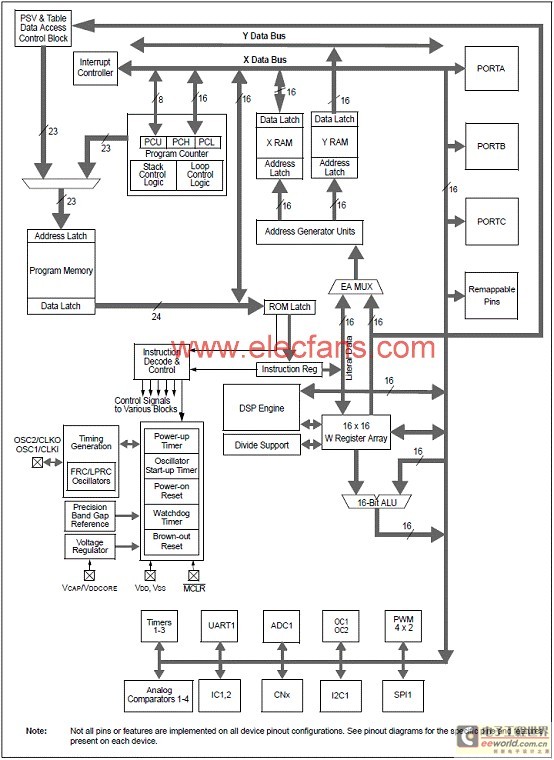
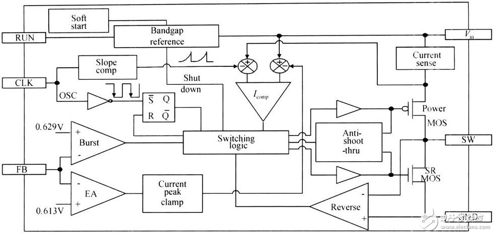
ͼ1��dsPIC33FJ06GS101/X02��dsPIC33FJ16GSX02/X04 ����ͼ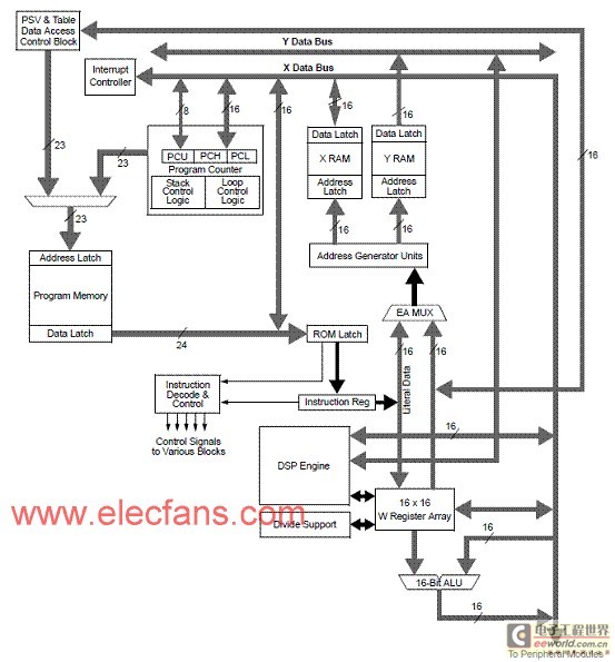
ͼ2��dsPIC33FJ06GS101/X02��dsPIC33FJ16GSX02/X04 CPU �˷���ͼ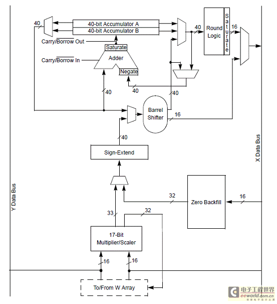
ͼ3��DSP ���淽��ͼ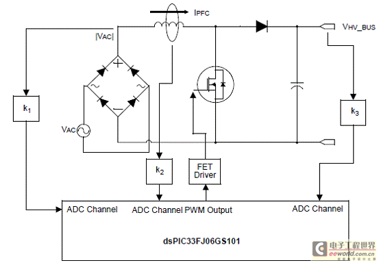
ͼ4��dsPIC33FJ ����PFC��ͼ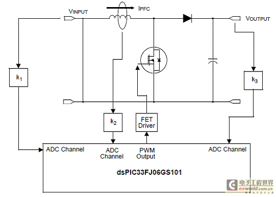
ͼ5��dsPIC33FJ ��ѹת������ͼ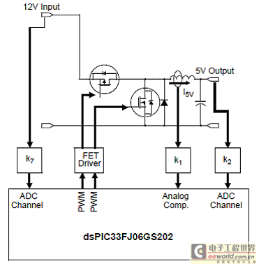
ͼ6��dsPIC33FJ ����ͬ����ѹת������ͼ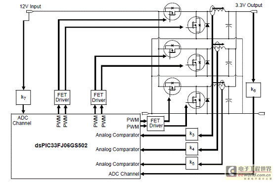
ͼ7��dsPIC33FJ ����ͬ����ѹת������ͼ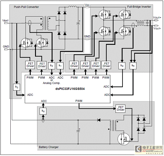
ͼ8��dsPIC33FJ ����UPS��ͼ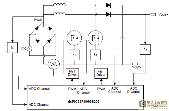
ͼ9��dsPIC33FJ ����PFC��ͼ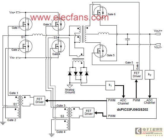
ͼ10��dsPIC33FJ ����ȫ�ţ�PSFB��ת������ͼ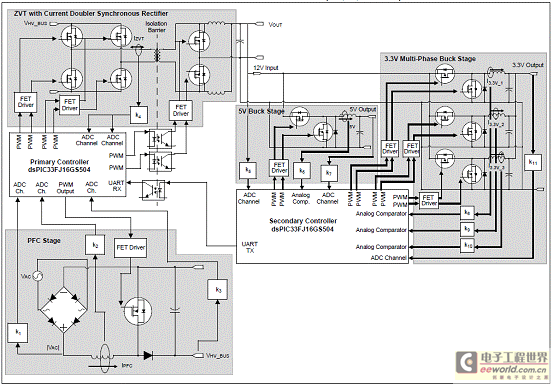
ͼ11����PFC�����(12V, 5V��3.3V)AC/DC��Դ��ͼ
1/4ש��DC/DCת�����ο����
Quarter Brick DC/DC Converter Reference Design
This reference design provides an easy method to evaluate the power, and features of SMPS dsPIC Digital Signal Controllers in high density quarter brick DC-DC converters for intermediate bus architectures(IBA). This reference design is implemented using a single dsPIC33F ��GS�� digital-power DSCs from Microchip that provides the full digital control of the power conversion and system management functions. As shown in this reference design the dsPIC33F ��GS�� devices enable designers to easily and cost effectively create products using advanced switching techniques such as Phase Shift Full Bridge (PSFB) topology that lower switching losses and enable efficiencies as high as 94%. The Quarter brick DC/DC Converter Reference Design is royalty free when used in accordance with the licensing agreement.
This reference design works with telecom input range 36V �C 76V DC and provides 12V with 200W power. Designed with planar magnetics, this reference design implements various non-linear techniques, which improves the performance and efficiency.
1/4ש��DC/DCת�����ο������Ҫ���ԣ�
Primary and Secondary MOSFET control
Active Current Share
Remote ON/OFF
Programmable soft start
Controlled Fall time
Voltage,Current,Temperature monitoring & Protection
Configurable output voltage
Full Digital Control
1/4ש��DC/DCת�����ο����ָ�꣺
Industry standard Quarter-brick (36.8 x 58.4 x 11.4 mm)
Wide input range 36V -76V
Output Voltage: 12V
Output Current: 17A
Output Power : 200W
Efficiency greater than 93%
1500 Vdc input to output isolation 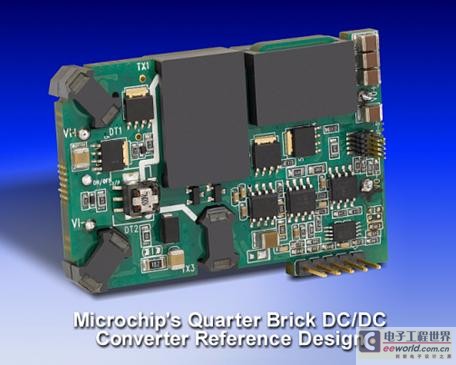
ͼ12��1/4ש��DC/DCת�����ο��������ͼ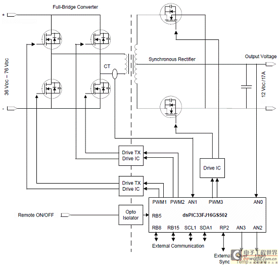
ͼ13��1/4ש��DC/DCת������dsPIC DSC��Դͼ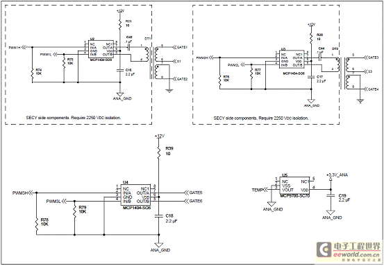
ͼ14��PSFB 1/4ש��DC/DCת������·ͼ��1��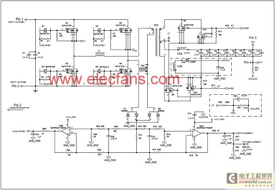
ͼ15��PSFB 1/4ש��DC/DCת������·ͼ��2��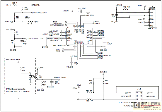
ͼ16��PSFB 1/4ש��DC/DCת������·ͼ��3��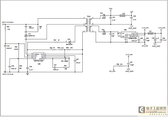
ͼ17��PSFB 1/4ש��DC/DCת������·ͼ��4��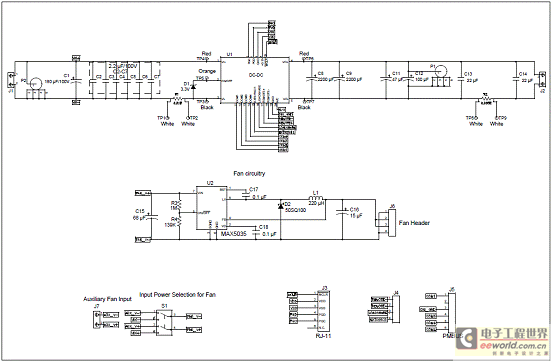
ͼ18�������·ͼ
�������������������������� �鿴���� �ظ�
"����dsPIC33FJ��Ƶ�PSFBש��DC-DCת�������� - ģ���Դ -"���������
��������
- ������ӱSH79F081�ĵ�Դ���������� - ģ���Դ -
- ����SP6641���ֳ��豸��Դ��� - ģ���Դ -
- ��������������������Դ�е�Ӧ�øĽ� - ģ���Դ
- ����߹����ܶȵĽ�ѹ��ѹ�� - ģ���Դ -
- �����ѹ������ȱ����� - ģ���Դ -
- PC����Դ�ڲ��ṹ���� - ģ���Դ -
- ����Ч�ȵ��ݹ����·��� - ģ���Դ -
- ���ʵ�жԵ�Դ�ĸ��� - ģ���Դ -
- ����AVR��Ƭ������Ƶ��Դ����ϵͳ - ģ���Դ -
- Ƕ��ʽϵͳ�����Դ��� - ģ���Դ -