电路简单双打输入频率-Simple Circuit Doub - 模拟电源 -
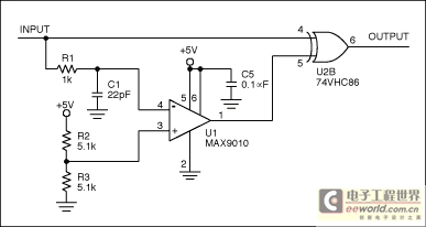
Figure 1. This circuit doubles the input frequency.
The reference frequency in this circuit drives the input of an exclusive-OR gate (XOR gate U2) as well as the input to a delay circuit. Consisting of R1, C1, and comparator U1, the delay circuit drives the XOR gate's second input. A resistive divider from the power supply establishes a 50% threshold for the delay circuit (2.5V in this case).
Circuit operation is easily illustrated by its response to a discrete pulse. If the input is low for a long time, pin 4 of the XOR gate is low but pin 5 is high, due to signal inversion by the comparator. The XOR output is therefore high. If the pin-4 input is now driven high, the XOR gate responds immediately by driving its output low. But after the delay circuit responds (about 15ns in this case), the XOR output returns high. Thus, a single rising edge on the input causes a single negative pulse at the XOR output. In a similar manner, the system produces a single pulse in response to an input falling edge. The resulting output (Figure 2) doubles an input frequency from 15MHz to 30MHz.
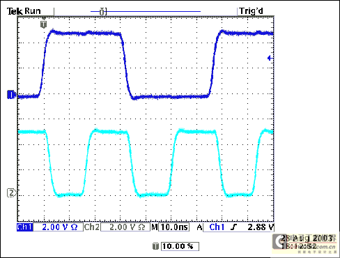
Figure 2. The Figure 1 circuit doubles a 15MHz input frequency+ to 30MHz.
A few simple selections configure this circuit for an application. The logic gate must operate from the desired supply voltage and provide adequate speed for the application. The delay components, R1 and C1, are determined by the equation
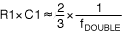
where fDOUBLE is the desired (doubled) output frequency. At higher frequencies R1 should be in the 1k range, but its value can be increased at lower frequencies. The calculated values of R1 and C1 may need adjustment to compensate for propagation delay in the comparator. Choosing a fast comparator (such as the MAX9010) helps to alleviate this concern. For low-level signals the MAX9010 propagation delay is 5ns, but a high level of overdrive in this application makes it faster than 5ns.
The circuit is useful in systems for which a clock frequency is already present, but other circuitry requires a higher frequency. Using a doubler instead of a second clock oscillator prevents the beat frequencies that might otherwise occur.
This design idea appeared in the December 15, 2003 issue of EE Times magazine.
查看评论 回复