IntroductionLow voltages are most appropriate for use in systems where size, weight, and power consumption are especially critical such as PDAs, cell phones, and other battery-operated portable equipment. Low voltages also benefit line-powered systems because the lower power dissipation associated with lower voltage operation allows the use of smaller power supplies, heat-sinks, and fans.
Low-voltage ICs are available in many of Maxim's product families including op amps, comparators, microprocessor supervisors, interface, data converters, analog switches and multiplexers, voltage references, DC-DC converters, digital potentiometers, and timing components such as real-time clocks.
This discussion covers many of the analog IC families mentioned above, the power savings inherent in their operation, and how to handle some of the issues associated with low-voltage operation. It also presents methods for generating the lower voltages from a 5V supply. Table 1 presents a selection of Maxim's 1.8V, 2.5V, 3.0V, and 3.3V integrated circuits.
Table 1. A Selection of Maxim's Low-Voltage Parts
| Category |
1.8V |
2.5V |
3V |
3.3V |
| P Supervisors |
MAX6326 |
MAX6742 |
MAX6745 |
MAX6745 |
| A/D Converters |
MAX1122 |
MAX1462 |
MAX1115 |
MAX1144 |
| Analog Switches |
MAX4695 |
MAX4644 |
MAX4653 |
MAX4592 |
| Charge-Pump Voltage Converters |
― |
MAX619 |
MAX1673 |
MAX1730 |
| Inductor-Based, Step-Up Regulators |
MAX1687 |
MAX1706 |
MAX1678 |
MAX1709 |
| Inductor-Based, Step-Down Regulators |
MAX1928 |
MAX1928 |
MAX1921 |
MAX1921 |
| Comparators, Fast |
LMX331 |
MAX997 |
MAX997 |
MAX997 |
| Comparators, Low Current |
MAX9020 |
MAX9020 |
MAX9020 |
MAX9020 |
| Comparators, Low Offset |
MAX966 |
MAX997 |
MAX997 |
MAX997 |
| D/A Converters |
MAX5522 |
MAX5523 |
MAX5811 |
MAX5355 |
| Digital Pots |
― |
DS4301 |
MAX5408 |
MAX5408 |
| Linear Regulators |
MAX1589 |
MAX1818 |
MAX1589 |
MAX1818 |
| Multiplexers |
MAX4638 |
MAX4638 |
MAX4639 |
MAX4701 |
| Op Amps, Fast |
MAX4291 |
MAX410 |
MAX4489 |
MAX4489 |
| Op Amps, Low Current |
MAX4036 |
MAX4036 |
MAX4036 |
MAX4036 |
| Op Amps, Low Offset |
MAX480 |
MAX4236A |
MAX4238 |
MAX4238 |
| Real-Time Clocks |
DS1375 |
DS1375 |
DS1375 |
DS1375 |
| References |
MAX6018A |
MAX6029 |
MAX6029 |
MAX6029 |
| RS-232 |
MAX218 |
MAX3381E |
MAX3322E |
MAX3232E |
| RS-485 |
― |
MAX3471 |
MAX3471 |
MAX3076E |
| USB |
MAX3453 |
MAX3453 |
MAX3453 |
MAX3453 |
Power Savings from Low-Voltage Operation
The power saved by reducing a system supply voltage from 5V to a lower value can be dramatic. For resistive and capacitive loads, power saved is proportional to the voltage squared. For constant-current loads such as references and op amps, the savings are linear. For constant-power loads such as hard-disk drives, the switch to low voltage does not save power, but requires the device to operate at a lower input voltage. Table 2 summarizes the power savings offered by lower voltage systems as compared to 5V systems.
Table 2. Power Savings Compared to 5V When Using Lower Voltages
| Load Type |
Power-Savings
Formula |
Power Savings Compared to 5V (%) |
1.8V
Operation |
2.5V
Operation |
3V
Operation |
3.3V
Operation |
| Resistive |
(1 - (V / 5)) x 100 |
87 |
75 |
64 |
56 |
| Capacitive |
(1 - (V / 5)) x 100 |
87 |
75 |
64 |
56 |
| Constant Current |
(V / 5) x 100 |
64 |
50 |
40 |
34 |
Voltage Regulation
General Information About Voltage Regulators
Maxim has scores of regulators that generate low voltage or convert low voltages to other levels. They include low-dropout linear regulators, switched-capacitor charge-pump converters, and inductor-based switching regulators.
Low dropout linear regulators (LDOs) are simple to use, require an input voltage greater than the output, and regulate up to 4A of output current. LDOs are less noisy and less expensive than switching regulators, but they dissipate more power (and generate more heat) as the applied input voltage rises. Linear regulators can, however, be quite efficient for applications with a low input-to-output voltage differential (efficiency is proportional to VOUT/VIN).
Charge-pump converters can boost a DC voltage to a higher value, or produce a voltage of opposite polarity from the input voltage. They use capacitors for energy storage and provide small, low-cost, DC-DC conversion circuits. However, they are limited in output current to less than 0.75A, and so they are restricted to low-power applications.
Inductor-based switching regulators offer both low- and high-power DC-DC voltage conversion, and can either step up (boost) or step down (buck) an input voltage. Maxim's boost regulators offer up to 4A of output current, and our buck regulators offer up to 60A of output current.
Low-Dropout Linear Regulators
Linear regulators require that the input voltage is greater than the output voltage. The minimum required difference between the input voltage and the output voltage is called the dropout voltage. Modern linear regulators have dropout voltages much lower than those of early linear regulators, like the LM7905, and have come to be called low-dropout regulators, or LDOs. Maxim offers a wide variety of LDOs with preset positive output voltages as low as 0.75V and adjustable voltages down to 0.5V. We also offer negative LDOs with outputs from -2.5V to -5V.
LDOs make regulating to a low DC voltage easy and economical. The MAX1589 LDO family is simple to use, feature preset output voltages that vary from 0.75V to 3.0V, and operate with less than 0.175V of dropout at their full 500mA of output current. The MAX1818 LDO family also offers preset output voltages from 0.75V to 3.0V, 500mA of output current, and feature adjustable output voltage down to 1.25V and a dropout voltage of only 0.12V at their full 500mA of output current.
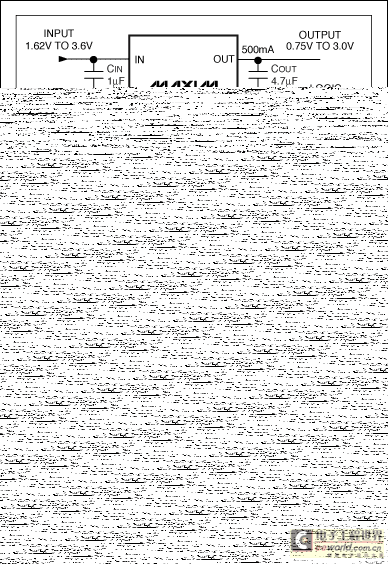
Figure 1. The MAX1589 500mA LDO has preset outputs of 0.75V, 1.0V, 1.3V, 1.5V, 2.5V, and 3.0V. The MAX1818 500mA LDO has preset outputs of 1.5V, 1.8V, 2.0V, 2.5V, 3.0V, and 5.0V or an adjustable output from 1.25V to 5V.
The MAX8510 LDO series incorporates several features important in the design of portable equipment: small size (SC70), low dropout voltage (120mV at 120mA), and low supply current (90A max.). The MAX8510/MAX8511 are preset to a variety of output voltages between 1.5V and 4.5V, while the MAX8512's output voltage can be adjusted with an external divider.
Charge-Pump Voltage Converters
For low-current applications, the simplest solution for boosting 3V to 5V is a capacitor-based regulating charge pump (Figure 2). The industry-standard 7660 and most other charge pumps don't regulate VOUT, but the MAX619 includes an analog reference and error amplifier whose output controls a set of internal switches connected to external capacitors. The switch-capacitor network can double or triple VIN, and the MAX619 regulates by switching between these modes of operation. As indicated, this circuit produces 20mA at 5V ±4% for inputs that range between 2V and 3.6V. For inputs between 3.0V and 3.6V, the output-current capability is 50mA.
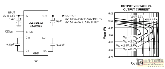
Figure 2. Occupying less than 0.1in of board space, the MAX619 regulated charge-pump converter generates 20mA at 5V ±4% for inputs of 2V to 3.6V and 50mA from 3V to 3.6V.
The MAX5008 regulated 5V USB charge pump provides an output current of up to 125mA with supply voltages down to 2.9V, and is suitable for USB host devices with 3.0V or 3.3V supplies.
Systems that handle bipolar signals usually require a negative supply, which can be generated locally if necessary. A simple solution is to use a charge-pump inverter such as the MAX889.
Inductor-Based, Switch-Mode Regulators
Switching regulators provide single or multiple outputs. Depending on the output power level, these devices are controlled by pulse-frequency modulation (PFM), pulse-width modulation (PWM), or both.. PFM control schemes, which allow high efficiency with light loads, permit the regulator to operate with quiescent supply currents as low as 10A. PWM schemes consume more power, but they allow fixed-frequency operation for better control of noise and EMI. Some converters switch between the two control schemes based on a control signal or the load-current level.
While LDOs are efficient for low values of (VIN - VOUT), many applications have an input voltage that is significantly higher than the output voltage. In this case, efficiency dictates the use of a buck-switching regulator. RF applications such as radios and cellular phones can easily use switching regulators, but care must be taken to avoid introducing noise at the sensitive IF frequencies.
An ideal choice for RF applications is the MAX1684 switching regulator. This device delivers 1A at 3.3V from inputs of 4V to 12V with efficiencies up to 97%, has a 300kHz internal oscillator, and features internal MOSFETs for ease of use.
An efficient buck regulator is also a good choice for upgrading an existing logic board to accommodate lower-voltage, lower-power ICs. These boards typically have 3.3V available, but they require a 1.8V supply for the new low-voltage logic. A linear regulator can easily convert 3.3V to 1.8V, but the power dissipation is prohibitive for higher load currents. At 2A, for instance, the linear regulator would dissipate 3W and require a heat-sink. The MAX1830 high-efficiency switcher (Figure 3), however, delivers 20mA to 2A with efficiencies exceeding 90% and requires no external MOSFETs, thus eliminating the need for a heat-sink.
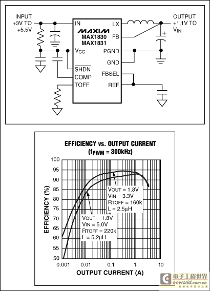
Figure 3. The MAX1830 switching regulator converts 3.3V to 1.8V with efficiency greater than 90% from 20mA to 2A, and requires no external MOSFETs.
The MAX1830 comes in a very small, 16-pin QSOP package and has an input range of 3V to 5.5V. Its quiescent operating current drops from 325A to only 0.2A in standby mode. High switching frequency (up to 1MHz) allows the device to operate with small, low-cost, surface-mount components.
Multi-output switching regulators are intended for systems designed to operate with multiple supplies. Applications such as the generation of VCC voltages in a notebook computer, for example, are well served by the MAX1999, which generates four regulated supply voltages (Figure 4).
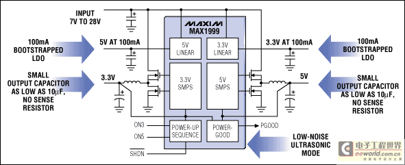
Figure 4. The MAX1999 switching regulator generates four output voltages and has two high-efficiency, high-power switch-mode regulators and two low-power linear regulators. It also includes a power-good output, shutdown control, current limiting, and pin-programmable power-up sequencing.
Data Converters
A/D Converters
Low power consumption is critical for A/D converters (ADCs) operating in portable equipment. These applications often require high speed, but high speed and low power tend to be mutually exclusive. Accordingly, Maxim produces ADCs that draw moderate supply currents while acquiring data, but very low currents while in shutdown. The result is a power savings for converters that need not operate continuously.
The MAX1115, for example, converts 100k samples per second. It operates from a +3V supply using only 175A of operating current, and uses just 1A of current in automatic power-down mode. The MAX1115 offers a large power savings for applications in which the sampling is intermittent (Figure 5).
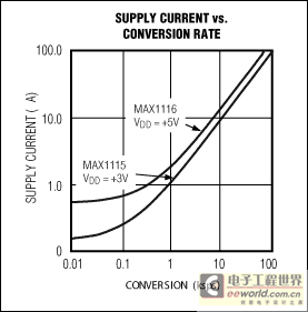
Figure 5. By entering a 1A power-down mode between conversions, the MAX1115 8-bit ADC offers a dramatic reduction in supply current.
One such application is the measurement of received signal strength in cellular telephones (RSSI: received signal-strength indicator). The MAX1115 digitizes the signal at 2ksps, while drawing a mere 2A from the 3V supply. Total unadjusted error (the sum of offset, integral nonlinearity, and gain errors) less than 1 LSB and SINAD (signal-to-noise and distortion) less than 48dB are guaranteed.
D/A Converters
Modern D/A converters (DACs) allow low-voltage digital systems to generate analog outputs. Intended for portable applications, these ICs require very little power and board area. The low-cost MAX5811, for instance, is a 10-bit, voltage-output DAC with low 170A operating current and just 1A shutdown current, which is ideal for portable applications. Its serial-data control allows it to fit into a SOT23 package.
The MAX5811 operates from single 2.7V supply, and its output swings rail-to-rail. It is ideal for low-cost applications such as trimming offset voltages, setting the bias point for adjustable current (or voltage) sources, and setting the regulation point in other circuits.
Op Amps and Current Monitors
In op amps, reduced-supply operation reduces the signal-to-noise ratio (SNR) by curtailing the output-voltage swing. Many low-voltage op amps, therefore, offer rail-to-rail output swings as a means of preserving the SNR. For the same reason, many feature an input-voltage range that includes one or both supply rails.
Low-voltage operation not only reduces the signal range, it puts an additional squeeze on SNR by raising the noise floor. Low-voltage amplifiers are often designed to draw low supply current, which leads to higher levels of amplifier noise. In addition, the feedback resistors have higher values (to limit system supply currents), which also adds noise.
To further complicate matters, high-impedance nodes are more likely to pick up noise from high-speed digital signals through capacitive coupling. Therefore, high-impedance traces should be kept short and physically distant from high-speed digital traces.
Noteworthy, and somewhat mutually exclusive, low-voltage op amp features include low supply current, low offset voltage, and high speed. The MAX4236A +3V series of devices, for example, combine a 1.7MHz gain-bandwidth product and 20V offset voltage with a low 350A supply current. Input common-mode voltage range is down to the negative rail, and the outputs swing rail-to-rail. These characteristics make the MAX4236A series of op amps useful as instrumentation amplifiers in low-voltage, battery-powered systems.
Maxim's op amp family also features bidirectional, high-side current-sense amplifiers, such as the +2.7V MAX4069 series (Figure 6). These current-sense amplifiers minimize grounding problems by employing high-side, current-sense resistors and come in 8-/10-pin MAX packages.
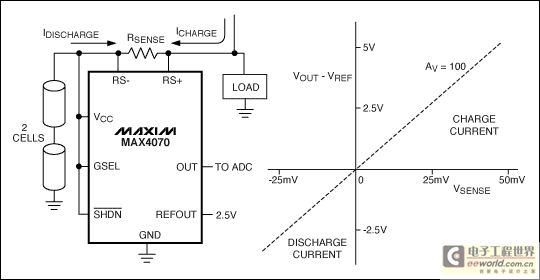
Figure 6. The MAX4070 bidirectional current-sense amplifier forms a complete current-to-voltage converter.
For portable applications that must conserve every microamp, some low-voltage, micropower op amps offer remarkably low supply currents. The +1.4V MAX4036/MAX4038 and +1.8V MAX4474 op amps offer extremely low power consumption at 1.2A (max). Outputs are rail-to-rail, and input ranges include the negative rail.
Input common-mode voltage range and output voltage swing typically become squeezed when powering op amps from low-voltage supplies. Care must be taken to observe these input and output limits when designing low-voltage circuits. Table 3 presents a cross section of data for the op amps discussed above.
Table 3. A Selection of Specifications for Some of Maxim's Low-Voltage Op Amps
查看评论 回复